


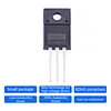


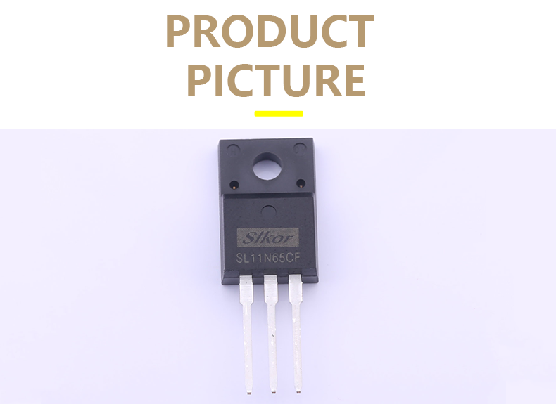
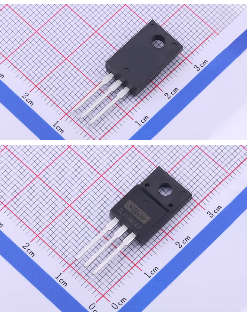
Xunster XST-MOS-L11N65CF n-channel super junction power semiconductor transistor
XST-MOS-L11N65CF
minimum order
1 piece
Quantity
- Model Number:XST-MOS-L11N65CF
- Type:MOSFET
- Place of Origin:Guangdong, China
- Brand Name:xunster
- Package Type:Surface Mount
- Supplier Type:Agency
- Media Available:datasheet
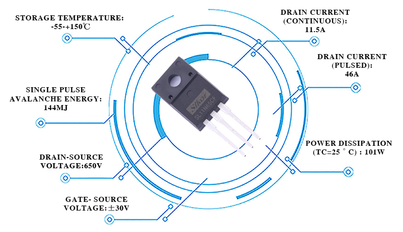
- Drain-Source Voltage (Vgs=0V):650V
- Gate-Source Voltage (Vds=0V), AC(f>1HZ):±30V
- Continuous Drain Current at Tc =25℃:11.5*A
- Continuous Drain Current at Tc =100℃:7*A
- Pulsed drain current (Note1):46*A
- Dissipation(Tc=25℃) Derate above 25℃:101 0.81"W W/℃"
- Single pulse avalanche energy(Note2):144mJ
- Avalanche current(Note1):6A
- tAR limited by Tjmax (Note 1):0.5mJ




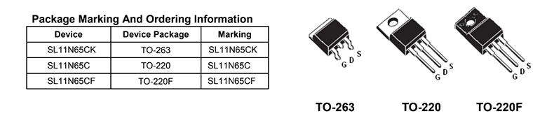
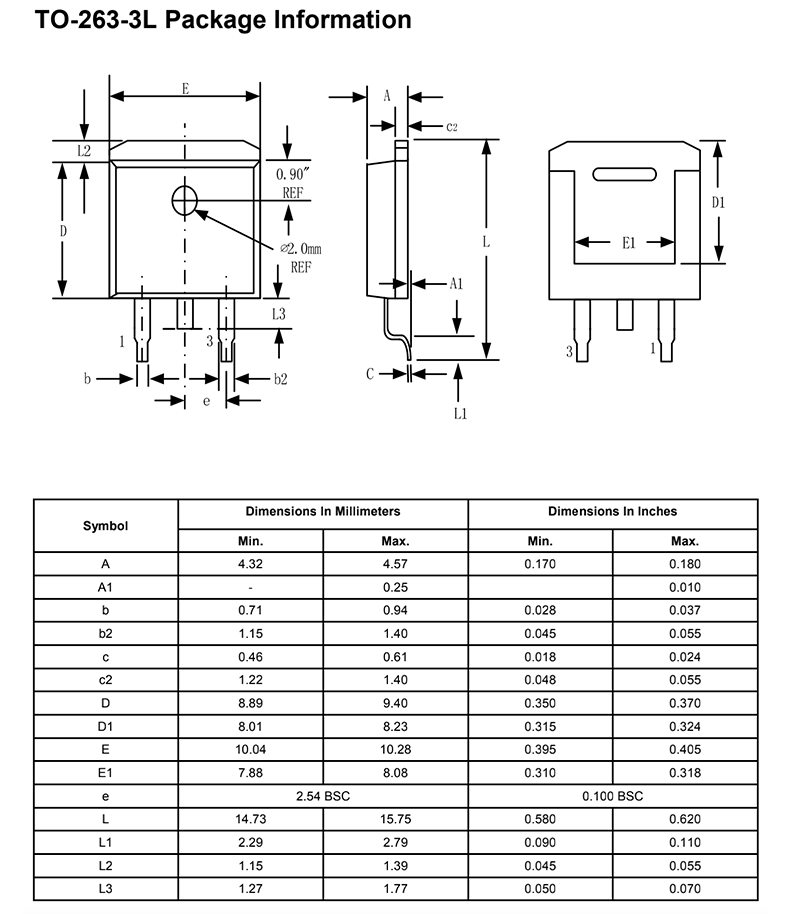
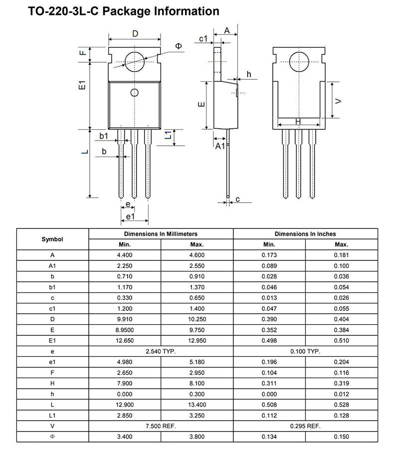
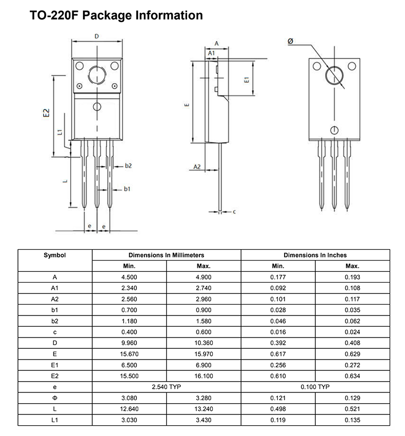
| Parameter | Symbol | SL21N65CK SL21N65C | SL21N65CF | Unit |
| Drain-Source Voltage | VDS | 650 | V | |
| Gate- Source Voltage | VGS | ±30 | ||
| Continuous Drain Current | ID @TC =25℃ | 11.5 | 11.5 | A |
| Continuous Drain Current | ID @TC =100℃ | 7 | 7 | |
| Pulsed Drain Current2 | IDM | 46 | 46 | |
| Maximum Power Dissipation(TC=25℃) Derate above 25°C | PD | 101 0.81 | 32.6 0.26 | W W/℃ |
| Single Pulse Avalanche Energy | EAS | 144 | mJ | |
| Avalanche Current | IAR | 6 | A | |
| Repetitive Avalanche energy ,tAR limited by TJmax(Note 1) | EAR | 0.5 | mJ | |
| Drain Source voltage slope, VDS ≤480 V | dv/dt | 50 | V/ns | |
| Reverse diode dv/dt,VDS ≤480 V,ISD | dv/dt | 15 | ||
| Operating Junction Temperature Range | TJ,TSTG | -55to+150 | ℃ | |
| Parameter | Symbol | Condition | Min | Typ | Max | Unit |
| On/off states | ||||||
| Drain-Source Breakdown Voltage | BVdss | Vgs=0V Id=250µA | 650 | V | ||
| Zero Gate Voltage Drain Current(Tc=25℃) | Idss | Vds=650V,Vgs=0V | 0.05 | 1 | µA | |
| Zero Gate Voltage Drain Current(Tc=125℃) | Idss | Vds=650V,Vgs=0V | 100 | µA | ||
| Gate-Body Leakage Current | Igss | Vgs=±20V,Vds=0V | ±100 | nA | ||
| Gate Threshold Voltage | VGS(th) | Vds-Vgs,Id-250µA | 3 | 3.5 | 4 | V |
| Drain-Source On-State Resistance | Rds(on) | Vgs=10V, Id=7A | 300 | 360 | mΩ | |
| Dynamic Characteristics | ||||||
| Input Capacitance | Clss | Vds=50V,Vgs=0V, F=1.0MHz | 870 | pF | ||
| Output Capacitance | Coss | 54 | PF | |||
| Reverse Transfer Capacitance | Crss | 1.8 | PF | |||
| Total Gate Charge | Qg | Vds=480V,Id=11.5A, Vgs=10V | 19 | nC | ||
| Gate-Source Charge | Qgs | 6 | nC | |||
| Gate-Drain Charge | Qgd | 6.5 | nC | |||
| Switching times | ||||||
| Turn-on Delay Time | td(on) | Vdd=380V,Id=5.5A, Rg=3oumiga,Vgs=10V | 11 | nS | ||
| Turn-on Rise Time | tr | 8 | nS | |||
| Turn-Off Delay Time | td(off) | 58 | 70 | nS | ||
| Turn-Off Fall Time | tf | 9 | 14 | nS | ||
| Source- Drain Diode Characteristics | ||||||
| Source-drain current(Body Diode) | Isd | Tc=25℃ | 11.5 | A | ||
| Pulsed Source-drain current(Body Diode) | Isdm | 46 | A | |||
| Forward on voltage | Vsd | Tj=25℃,lsd=11.5A,Vgs=0V | 0.9 | 1.2 | V | |
| Reverse Recovery Time | trr | Tj=25℃ IF=5.8A, di/dt=100A/µS | 220 | nS | ||
| Reverse Recovery Charge | Qrr | 2.2 | uC | |||
| Peak Reverse Recovery Current | Irrm | 19 | A | |||
Comprehensive score