





XST-IGBT-CMS6126 power transistor insulated gate bipolar transistor semiconductor
XST-IGBT-CMS6126
minimum order
1 piece
Quantity
- Model Number:XST-IGBT-CMS6126
- Type:Other
- Place of Origin:Guangdong, China
- Brand Name:xunster
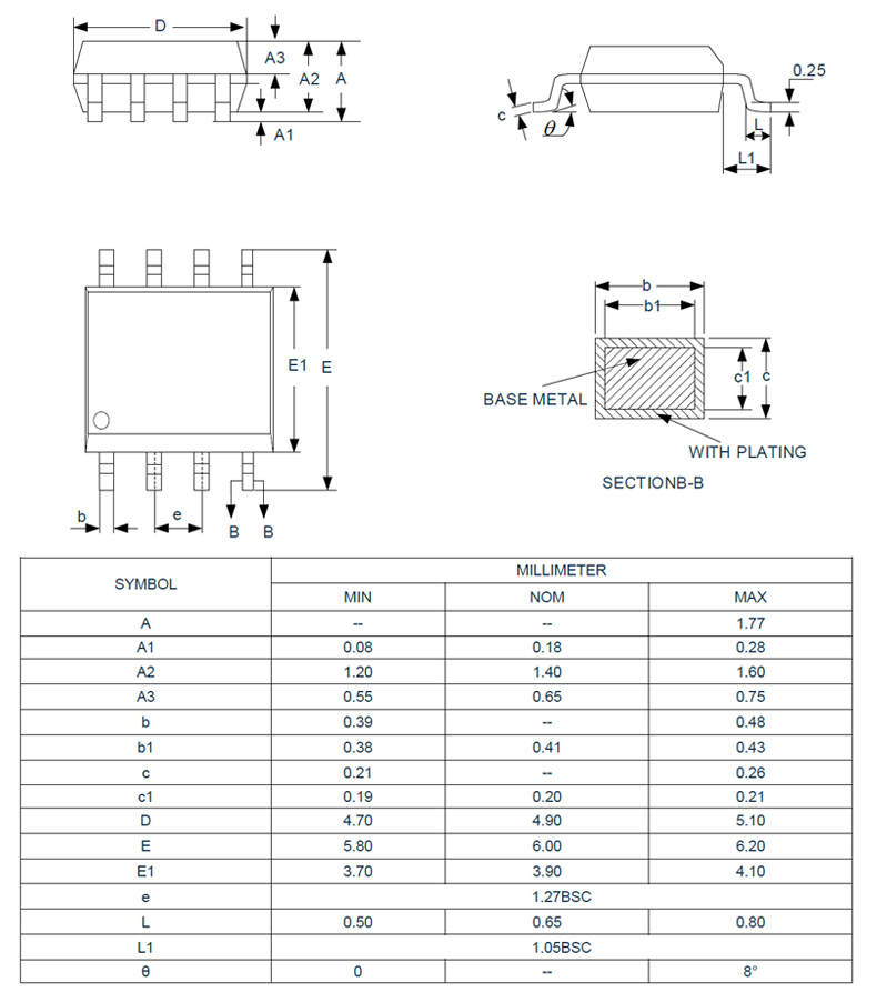
- Package Type:Surface Mount
- Supplier Type:Agency
- Media Available:datasheet
- High side floating absolute voltage:625V
- High side floating supply offset voltage:VB+0.3V
- High side floating output voltage:VB+0.3V
- Low side and logic fixed supply voltage:25V
- Low side output voltage:VCC+0.3V
- Logic input voltage (HIN & LIN):10V
- voltage transient:50 V/ns
- Package power dissipation @ TA ≤ +25°C:1W
- junction to ambient:125 °C/W
- Junction temperature:300°C
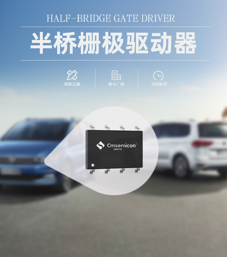

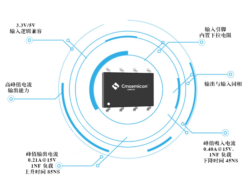
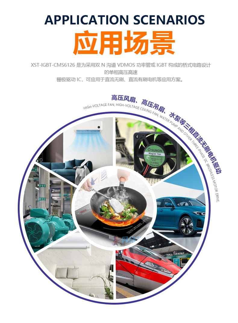
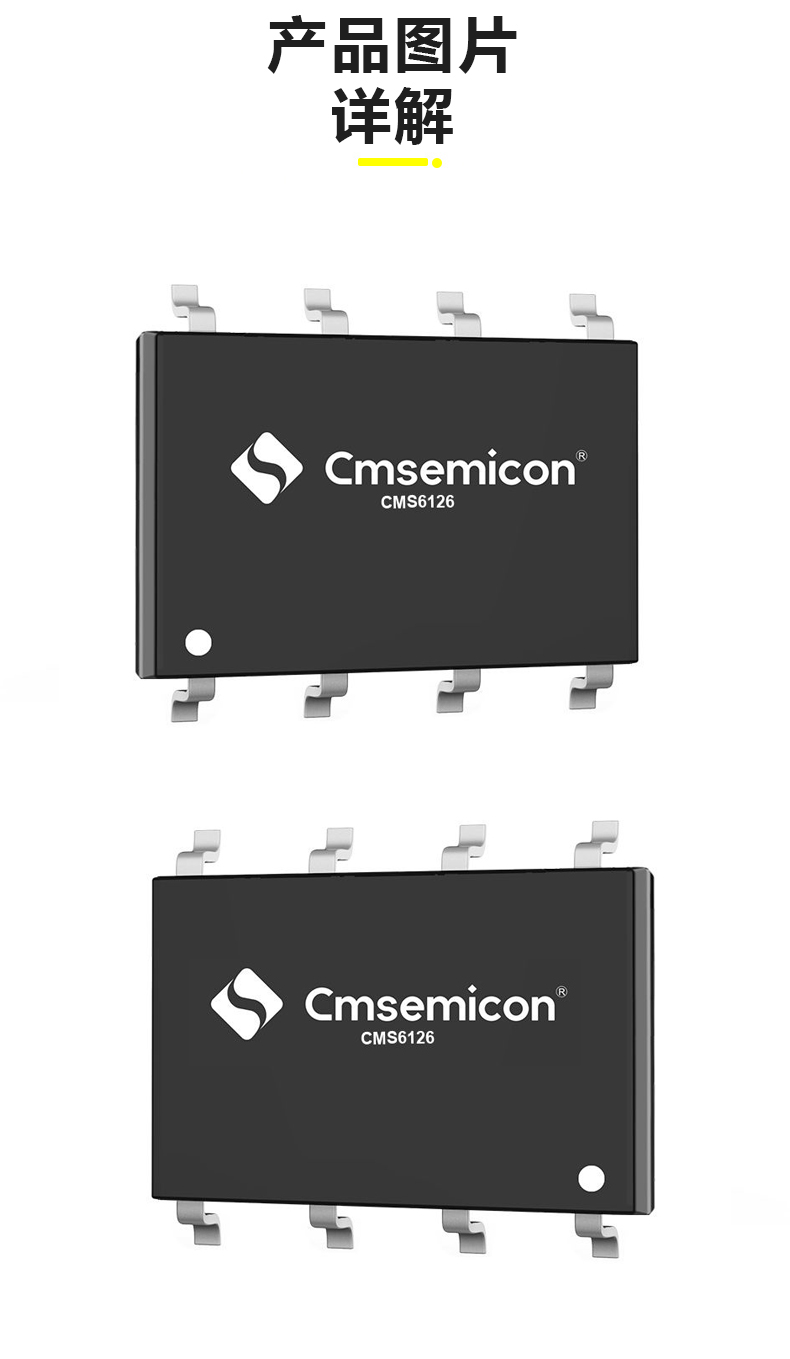
Cms6126 is a single-phase high-voltage high-speed gate drive IC designed for bridge circuit composed of double n-channel VDMOS power transistor or IGBT. It can be applied to applications such as DC brushless motor and DC brushless motor. Cms6126 controls the high side drive circuit output (HO) and low side drive circuit output (LO) respectively through input signals (hin and Lin). The built-in 320ns dead time is the minimum dead time. When the dead time of the MCU output signal is greater than the built-in dead time, the actual dead time is the dead time set by the MCU. Built in VCC and VBS undervoltage (UVLO) protection function can prevent the system from opening the external power tube at low driving voltage.


| (TA = 25 ℃, VM = 12V, nu = NV = NW = GND, all pins take GND as the reference point, unless otherwise specified) | ||||||
| parameter | Sign bit | Test conditions | minimum value | Typical value | Maximum | Company |
| Power supply current parameters | ||||||
| VCC quiescent current | ICCQ | VHIN=VLIN=0 | - | 175 | - | uA |
| VBS quiescent current | IBSQ | VHIN=0 | - | 60 | - | uA |
| VCC dynamic current | ICCD | fLIN=20kHz | - | 250 | - | uA |
| VBS dynamic current | IBSD | fHIN=20kHz | - | 165 | - | uA |
| Leakage current of VB floating power supply | ILK | VB=VS=600V | - | 1 | 5 | uA |
| Power supply voltage parameters | ||||||
| VCC Undervoltage high level potential | VCCHY+ | - | 8.8 | - | V | |
| VCC Undervoltage high level potential | VCCHY- | - | 8.2 | - | V | |
| VCC Undervoltage hysteresis level | VCCHY | 0.4 | 0.6 | - | V | |
| VBS Undervoltage high level potential | VBSHY+ | - | 8.8 | - | V | |
| VBS Undervoltage high level potential | VBSHY- | - | 8.2 | - | V | |
| VBS Undervoltage hysteresis level | VBSHY | 0.4 | 0.6 | - | V | |
| VS Static negative pressure | VSQN | VBS=15V | - | -5 | - | V |
| Time parameter | ||||||
| When the rising edge of the output is transmitted | ton | No Load | - | 320 | - | ns |
| Output falling edge transmission time | toff | No Load | - | 320 | - | ns |
| Output rise time | tr | CL=1nF | - | 85 | 125 | ns |
| Output falling time | tf | CL=1nF | - | 45 | 70 | ns |
| Dead Time | DT | No Load | - | 320 | - | ns |
| High and low side matching time | MT | TON & TOFF | - | - | 50 | ns |

Comprehensive score