





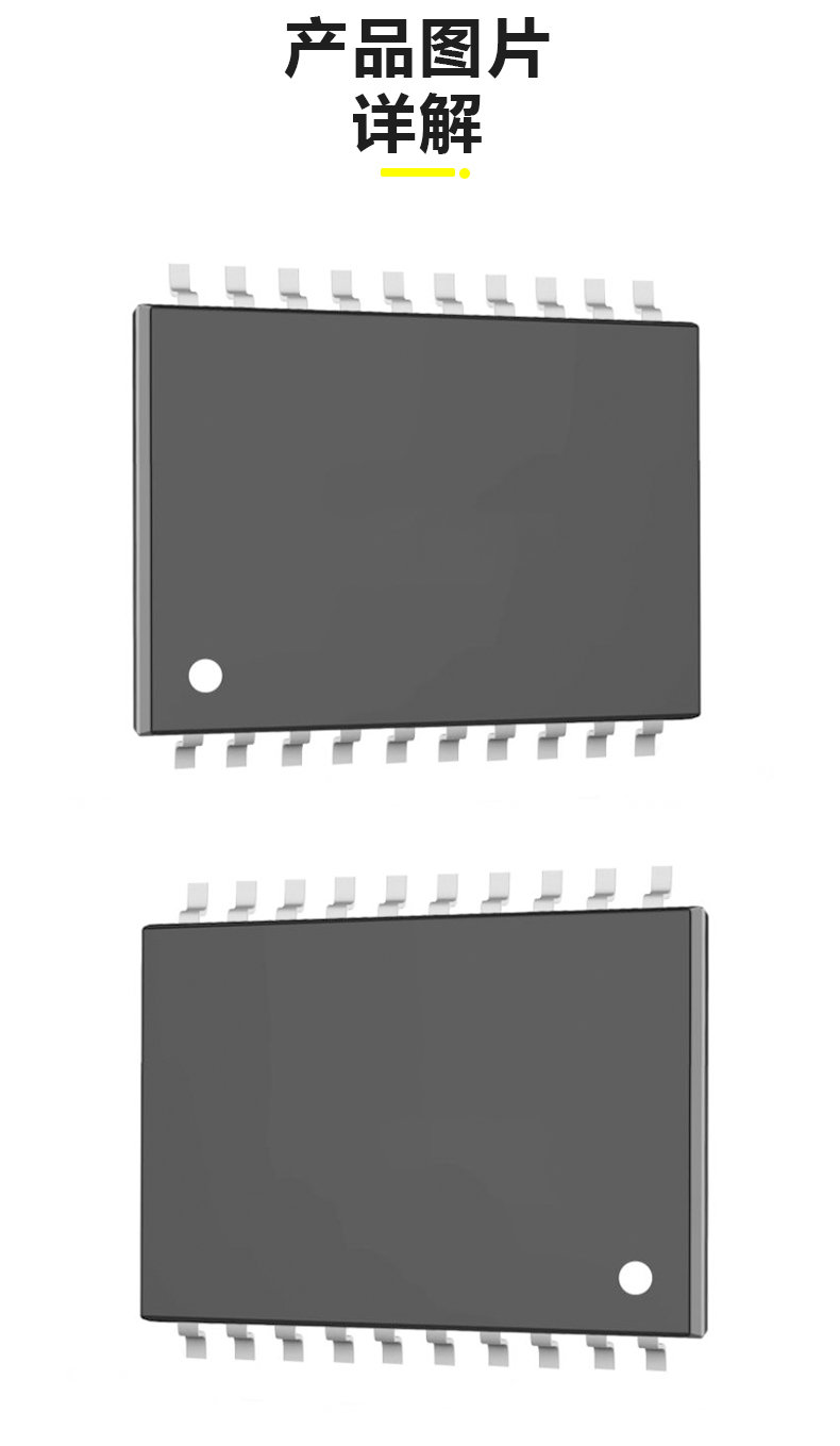
Insulated Gate Bipolar Transistor XST-IGBT-CMS6163N IGBT semiconductor
XST-IGBT-CMS6163N
minimum order
1 piece
Quantity
- Model Number:XST-IGBT-CMS6163N
- Type:Other
- Place of Origin:Guangdong, China
- Brand Name:xunster
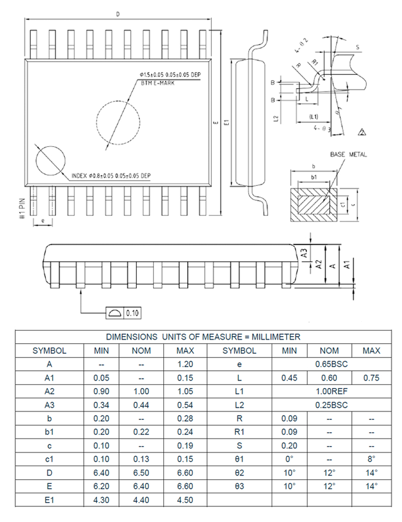
- Package Type:Surface Mount
- Supplier Type:Agency
- Media Available:datasheet
- High side absolute voltage:VS1,2,3+25V
- High side relative voltage:180V
- High side output voltage:VB1,2,3+0.3V
- Maximum supply voltage:25V
- Low side output voltage:VCCV
- Junction temperature:150℃
- Storage temperature:150℃
- Maximum power consumption (Note 1):1.25W
- Pin welding temperature (duration 10s):260℃
- ESD (Note 2):2000V
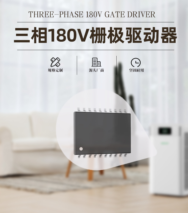

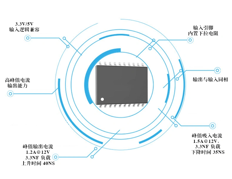
Xst-igbt-cms6163n controls high side drive circuit output (HO) and low side drive circuit output (LO) respectively through input signals (hin and Lin). The built-in 200ns dead time is the minimum dead time. When the dead time of the MCU output signal is greater than the built-in dead time, the actual dead time is the sum of the dead time set by the MCU and the built-in dead time. Built in VCC and VBS undervoltage (UVLO) protection function can prevent the system from opening the external power tube at low driving voltage.



| (TA = 25 ℃, VM = 12V, nu = NV = NW = GND, all pins take GND as the reference point, unless otherwise specified) | ||||||
| parameter | Symbol | Test conditions | minimum value | Typical value | Maximum | Company |
| Power supply current parameters | ||||||
| VCC Quiescent current | ICCQ | VIN=0V | - | 160 | 280 | uA |
| VBS Quiescent current | IBSQ | VHIN=0V | - | 120 | 180 | uA |
| VCC Dynamic current | ICCD | fLIN1,2,3=20kHz | - | 250 | 380 | uA |
| VBS Dynamic current | IBSD | fHIN1,2,3=20kHz | - | 220 | 380 | uA |
| VB Floating power leakage current | ILK | VB1,2,3=VS1,2,3=180V | - | 0.1 | 10 | uA |
| Power supply voltage parameters | ||||||
| VCC Undervoltage high level potential | VCCHY+ | 5.8 | 6.4 | 7 | V | |
| VCC Undervoltage high level potential | VCCHY- | 5.4 | 6 | 6.6 | V | |
| VCC Undervoltage hysteresis level | VCCHY | 0.4 | 0.4 | 0.4 | V | |
| VBS Undervoltage high level potential | VBSHY+ | 5.8 | 6.4 | 7 | V | |
| VBS Undervoltage high level potential | VBSHY- | 5.4 | 6 | 6.6 | V | |
| VBS Undervoltage hysteresis level | VBSHY | 0.4 | 0.4 | 0.4 | V | |
| VS Static negative pressure | VSQN | VBS=15V | - | -8 | -10 | V |
| Time parameter | ||||||
| When the rising edge of the output is transmitted | ton | No Load | - | 300 | 400 | ns |
| Output falling edge transmission time | toff | No Load | - | 100 | 150 | ns |
| Output rise time | tr | CL=3.3nF | - | 40 | 70 | ns |
| Output falling time | tf | CL=3.3nF | - | 35 | 60 | ns |
| Dead Time | DT | No Load | 100 | 200 | 300 | ns |
| High and low side matching time | MT | - | - | 30 | ns | |

Comprehensive score